TEM Hardware
16 Apr 2025The first time I met a transmission electron microscope (TEM) I was surprised at how tall it was, rising far over our heads. Behind it pumps, computers, and a forest of cables typing everything into a working instrument. I thought: “Why does it take up an entire room? What does all of it do?” I think a lot of people have a similar reaction, the sheer size of the machine demanding an explanation of it’s purpose and function.
The bright spark infusing life into a TEM is the electron source, without which the microscope would be so much scrap. Perching at the column’s peak, an electron gun emits and accelerates a beam of electrons. We often control the accelerating voltage, the kinetic energy of our electrons in kilo electron volts. Higher voltage gives faster electrons with smaller wavelength – a 200 keV electrons’ wavelength is 0.00251 nm, while visible light is hundreds of nanometres. For microscopy we want the beam monochromatic and bright, so a small range of wavelengths and the beam emitted through a small angle range.
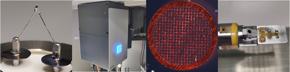
Inside the gun electrons are emitted into vacuum so we can apply acceleration. The simplest method is heating a material above it’s work function (at which point it will start spraying electrons out like a shaken-up drink can) the principle behind thermionic emission. Cheap thermionic sources are a bent tungsten wire, and expensive sources are lanthanum hexaboride crystals (LaB6); with cost similar to a cup of nice coffee or an old used car respectively. LaB6 crystals, which are a lovely purple colour, emit electrons from a smaller area and work at a lower temperature than tungsten hairpins, so they have better spatial coherency and are more monochromatic. Better than thermionic are Schottky sources, where a sharp oriented tungsten crystal has it’s work function lowered by a layer of semiconductor and the presence of an electric field to enhance thermionic emission, but we use a field-emission gun (or FEG) for the brightest and most monochromatic beams. Here a sharp tungsten crystal is placed into a strong electric field causing electrons to tunnel from the tip – no heating required. I find it interesting that FEGs have smaller beam current than thermionic sources but are brighter, as they emit through a smaller angle range.
As a potter works raw clay emitted beams are shaped and guided in the column by electron lenses. They let us create magnified images and often dictate the resolution, the smallest distance we can usefully observe. Electromagnetic lenses look very different to their glass counterparts; a soft iron polepiece guides the magnetic field made by the coils of copper wire surrounding it. To stop resistive heating could affect the magnetic field lenes are actively cooled. Electrons travel through the bore of the polepiece steered by the magnetic field – the field is stronger away from the centre of the bore, allowing us to focus the beam to a point. The focal length of the lens (where electrons are focussed to a point) is controlled by field strength, which we can affect by changing the current in the copper coils. Some lenses have multiple polepieces to remove optical aberrations by changing the beam’s shape. To further shape the beam we can physically block it with apertures. They’re often a strip of metal (a diaphragm) with a series of four or five apertures of decreasing size machined into it.
When the electrons pass through the sample they form an image of it, invisible to our eyes but not to our detectors. First is a phosphor viewing screen that glows green when illuminated with electrons; below that a digital camera, to convert the incoming electrons to a picture on a computer screen. Images are greyscale – darker areas mean less electron wave intensity, lighter areas more. Cameras might convert electrons into photons that are counted, such as complementary metal-oxide semiconductor (CMOS) detectors, while some of the newest cameras detect electrons directly. For spectroscopy, we have other detectors – the energy dispersive X-ray spectroscopy (EDS) detector is above the sample, picking up X-rays emitted from it when the beam passes through. Samples are put onto TEM grids, of which there are different types. For routine work we often use an electron transparent film of carbon, some twenty nanometres thick, on top of a small copper mesh disc. We can see the disc to handle it (gently) with tweezers, even if we can’t see nanoscale pieces of matter we’ve deposited onto the carbon film. The grid attaches to the holder, a long metal rod which is easier to handle than a grid, which we insert through an airlock into the imaging chamber. Everything we’ve discussed so far happens under vacuum, as trying to emit from a high voltage source through atmosphere would destroy or damage the instrument. Even below atmospheric pressure too much gas in the column causes poor performance from contamination build-up. Hence the airlock to insert the sample, reducing the gas volume we have to pump out when we want to change samples. To get a good vacuum (around 10-5 Pa or better) we have a series of pumps working together; an ion pump’s exhaust may be handled by a diffusion pump, in turn handled by a rotary pump that exhausts to the atmosphere. The best vacuum is in the gun, while the detector chamber has a slightly worse vacuum.
These are the main elements making up the microscope; source, lenses, detectors, sample, and vacuum. For deeper understanding there are plenty of textbooks and old hands to consult, and getting your hands dirty operating the microscope will do wonders. Microscopy requires the impetus of your scientific curiosity to make the beam useful, without it the TEM is silent.
Further Reading
Williams DB, Carter CB. Transmission Electron Microscopy: A Textbook for Materials Science. 2nd ed. New York: Springer; 2008. Chapters 6-8. p. 67-129.
Kirkland AI, Chang SL-Y, Hutchinson JL. Atomic Resolution Transmission Electron Microscopy. In: Hawkes P, Spence J, editors. Springer Handbook of Microscopy. Cham: Springer International Publishing; 2019. p. 3-48.
Acknowledgements
Thanks to the Nanoscale and Microscale Research Centre access to transmission electron microscopy equipment; and thanks to M Fay and I Cardillo-Zallo for input on technical content.